Reverse Engeneering an X-Ray generator - Part 1
Introduction
So I wanted to try reverse engeneering for a while now, so I finally found a project to work on: an X-Ray generator control board.
Let’s start
And what better way to go about that than an X-Ray image of this exact board? Since it’s a 4 layer PCB that’s really handy:
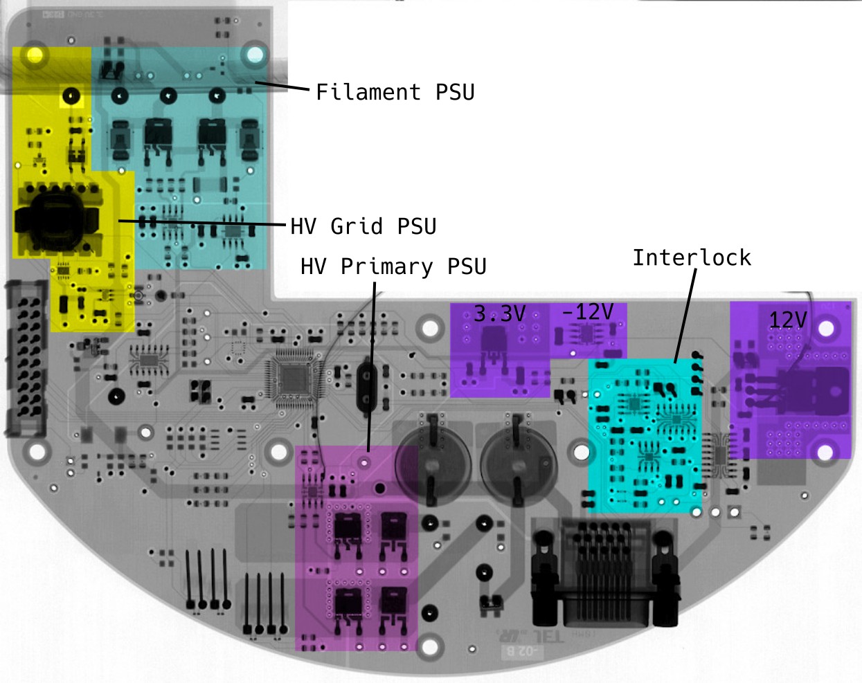
I thought about using inkscape for marking all traces and reconstructing a schematic that way, but I discarded that Idea fast, because that was just tedious work. I quickly switched to using KiCAD in a sort of “going back and forwarth” way - inserting an IC in the schematic - selecting the footprint - adding the footprint to the right place and then looking what connects to what.
Pinout
The connector is a DB-15 high density (3 row) connector, normally known for VGA. Unfortunately, you can’t use a VGA cable because it’s the wrong gender. I got my connector from a VGA to DVI adapter I cut apart for this project.
| Pin | Function |
|---|---|
| 1 | +24V |
| 2 | GND |
| 3 | GND |
| 4 | Enable Grid Supply |
| 5 | PC-14 STM32 |
| 6 | +24V |
| 7 | +24V |
| 8 | GND |
| 9 | Interlock |
| 10 | PC-15 STM32 |
| 11 | RS232 Rx |
| 12 | NC |
| 13 | GND |
| 14 | RS232 Tx |
| 15 | NC |
Interlock circuitry:
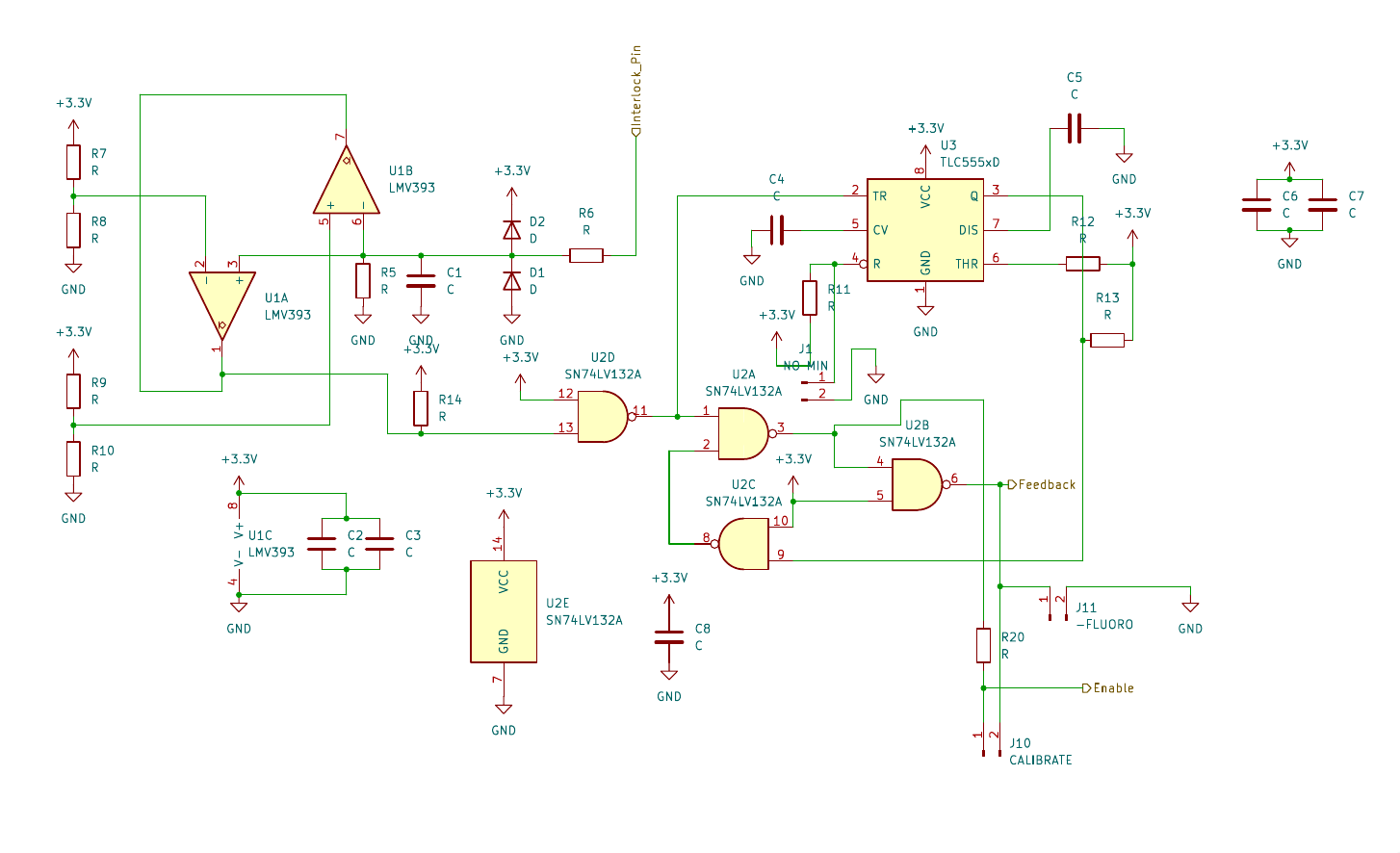
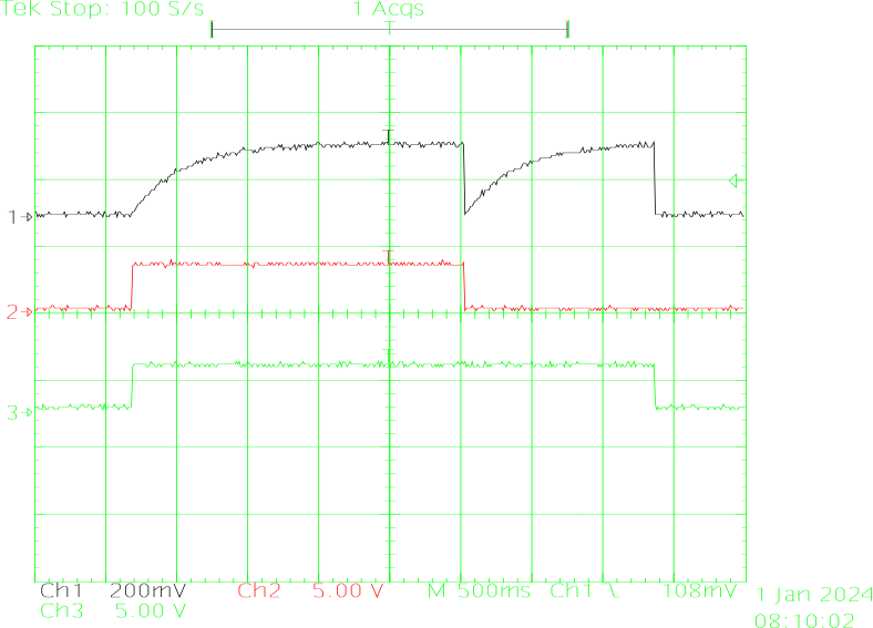
The LMV393 Opamp checks if the input is between 1V and 2V, only then this signal is then passed on to the SN74LV132A quad NAND gate where it is combined with a TLC555 timer which is configured in a way to set a minimum on time, it can be best grasped with the oscilloscope traces (1: Voltage on capacitor, 2: input from OpAmp output, 3: Enable Out):
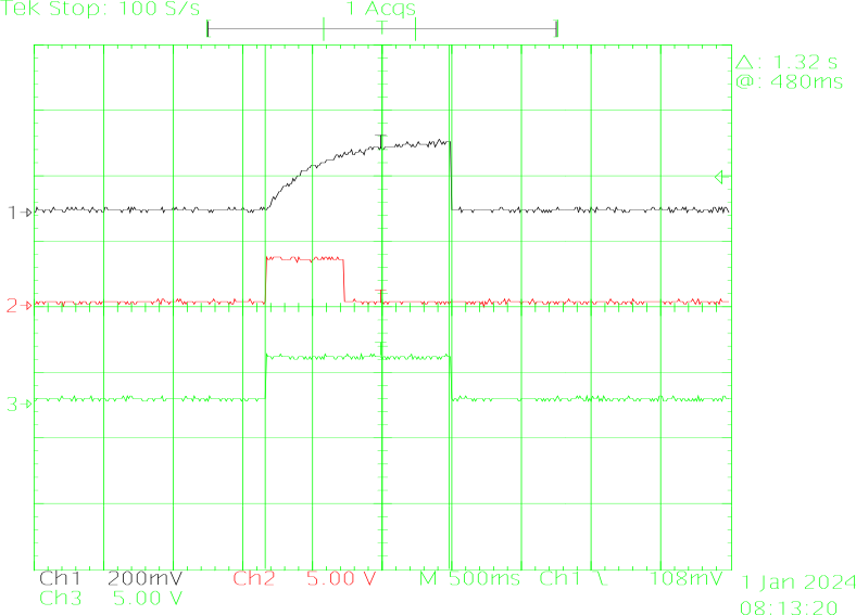
The Jumper labeled “NO MIN” will disable this minimum on duration.
There are 2 outputs from this signal: The one labeled “Enable” in my schematic will head on to the HV Primary PSU side and enable the Mosfet Driver (active high). The other output labeld “Feedback” heads to the STM32F103RCT - Pin PA-3.
Power Rails
This PCB has a few power rails and a quite interesting distribution technique. The main voltages (distributed via an inner layer) are:
- 3.3V
- 12V
additionally:
- 24V
- -12V
The 3.3V is distributed via the same inner layer as the 12V rail. It is split in 2 parts - red area is supplied with 12V, blue area with 3.3.

HV Grid supply
For the grid a high, negative voltage is needed, this is generated by using a MAX13256 H-Bridge Transformer Driver.
For it to be enabled, the MCU has to pull it’s enable line on PC7 high as well as the Pin 4 on the DB-15 connector has to be pulled high (3.3V).
Filament PSU and HV Primary PSU
Those are quite similar. They both use a mosfet driver, a halve H bridge and Diodes to protect against negative voltage spikes.
Jumper functions
| Jumper | Label | Function |
|---|---|---|
| JP1 | Pulls PA-8 low | |
| JP2 | Pulls PC-9 low | |
| JP3 | FLUORO- | Hard pulls interlock output low |
| JP4 | CALIBRATE | Pulls Feedback and enable together |
| JP5 | NO MIN | Pulls the Reset of timer (for interlock delay) low, disableing it |
Potentiometer (R54) function
This potentiometer calibrates the voltage devider for HV measurment.
Next steps
I also want to try reverse engeneering the software. Stay tuned for that!
Please reach out to me via mail if you need the full schematic and PCB design.